二手 VON ARDENNE WM70H / C #9172921 待售
网址复制成功!
单击可缩放



















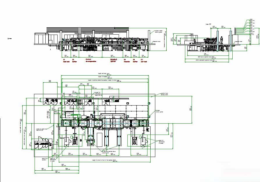

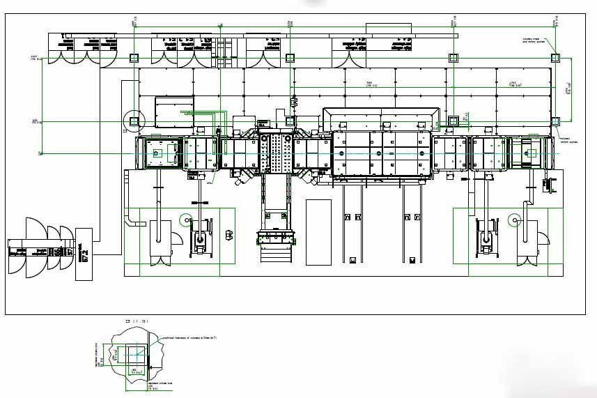


ID: 9172921
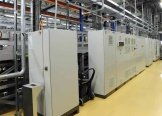
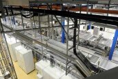
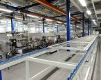
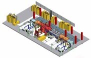
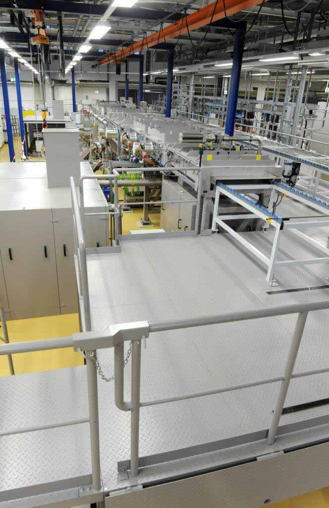
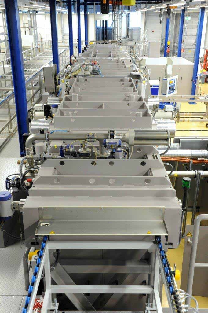
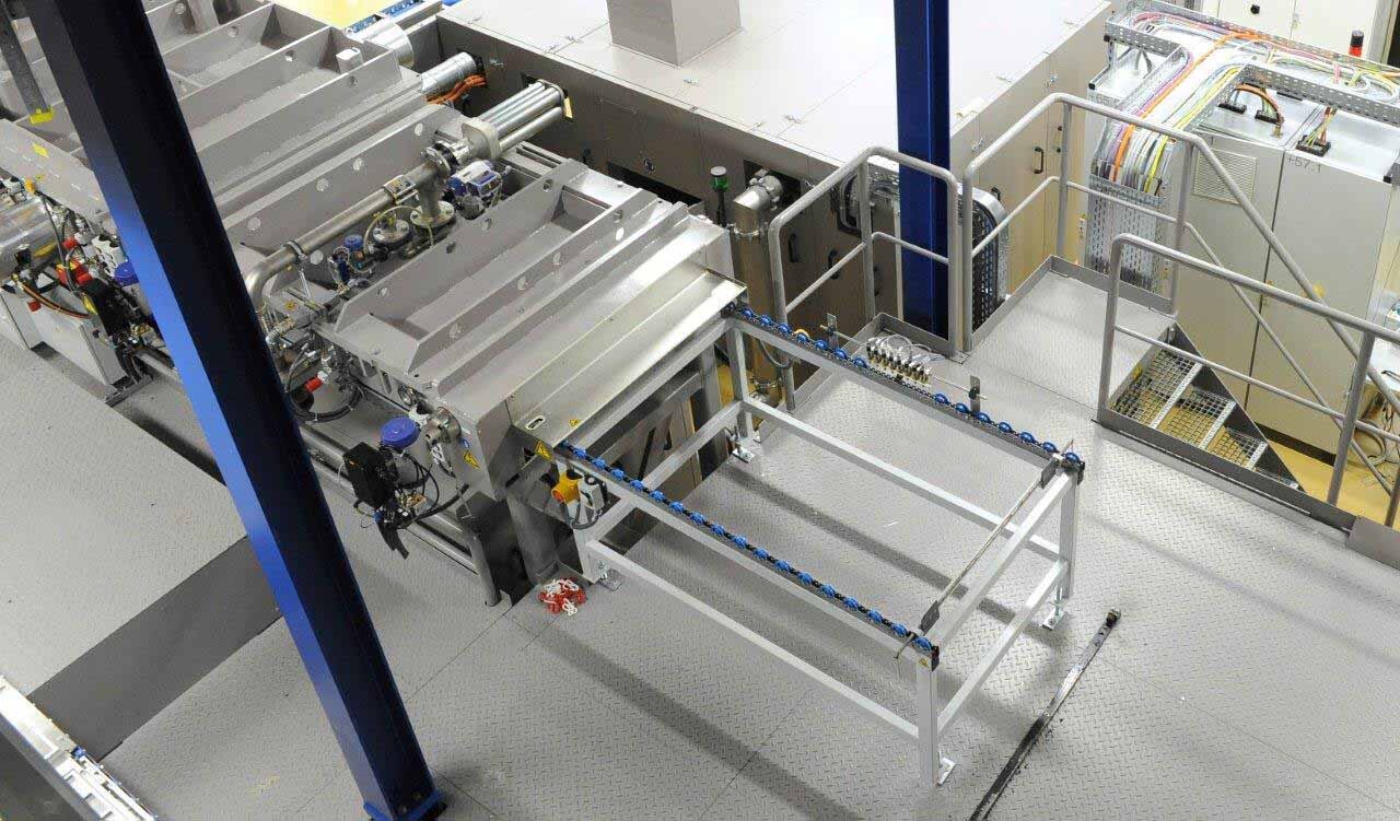
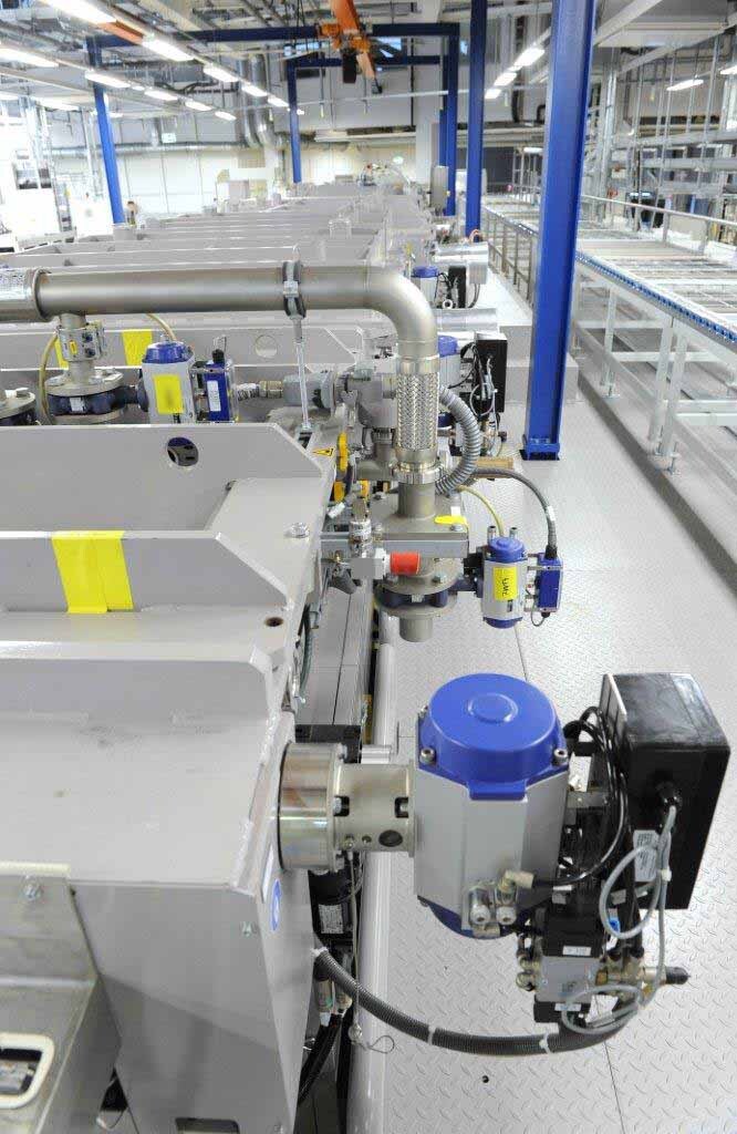
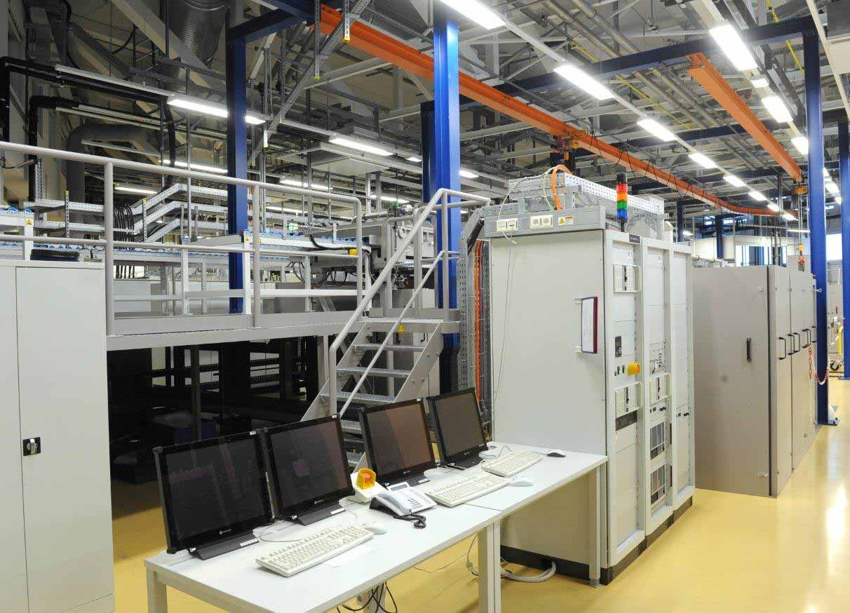
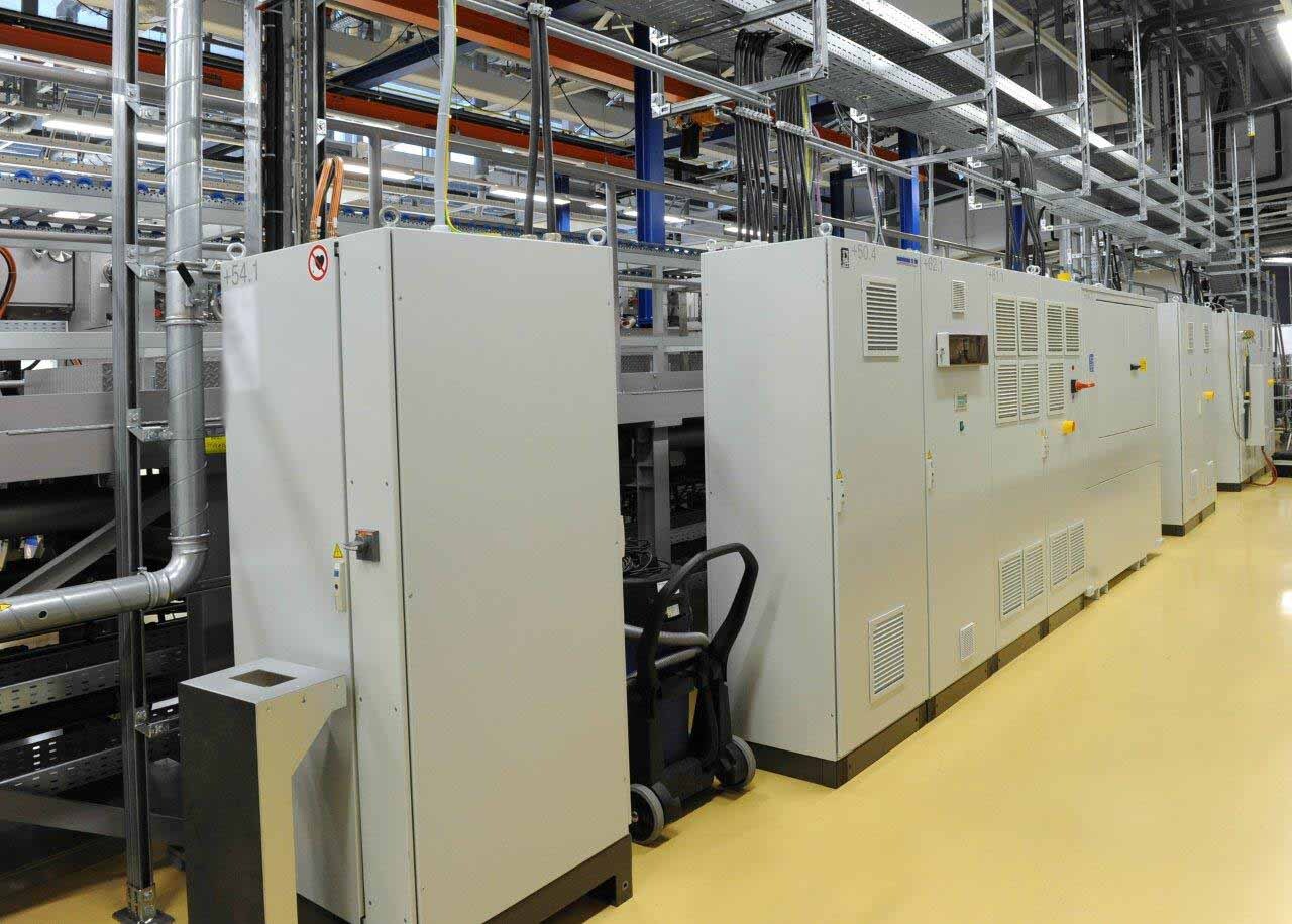
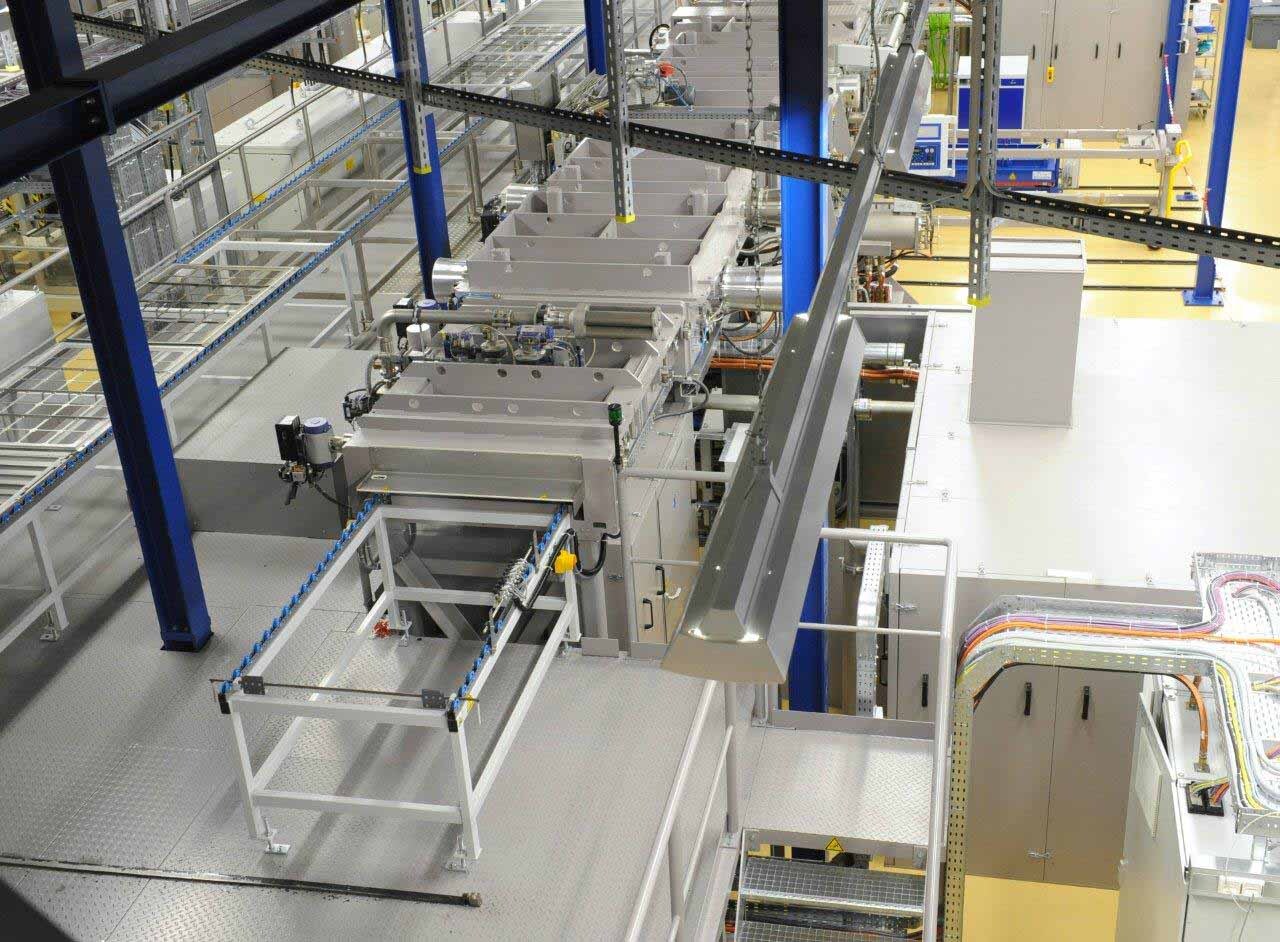
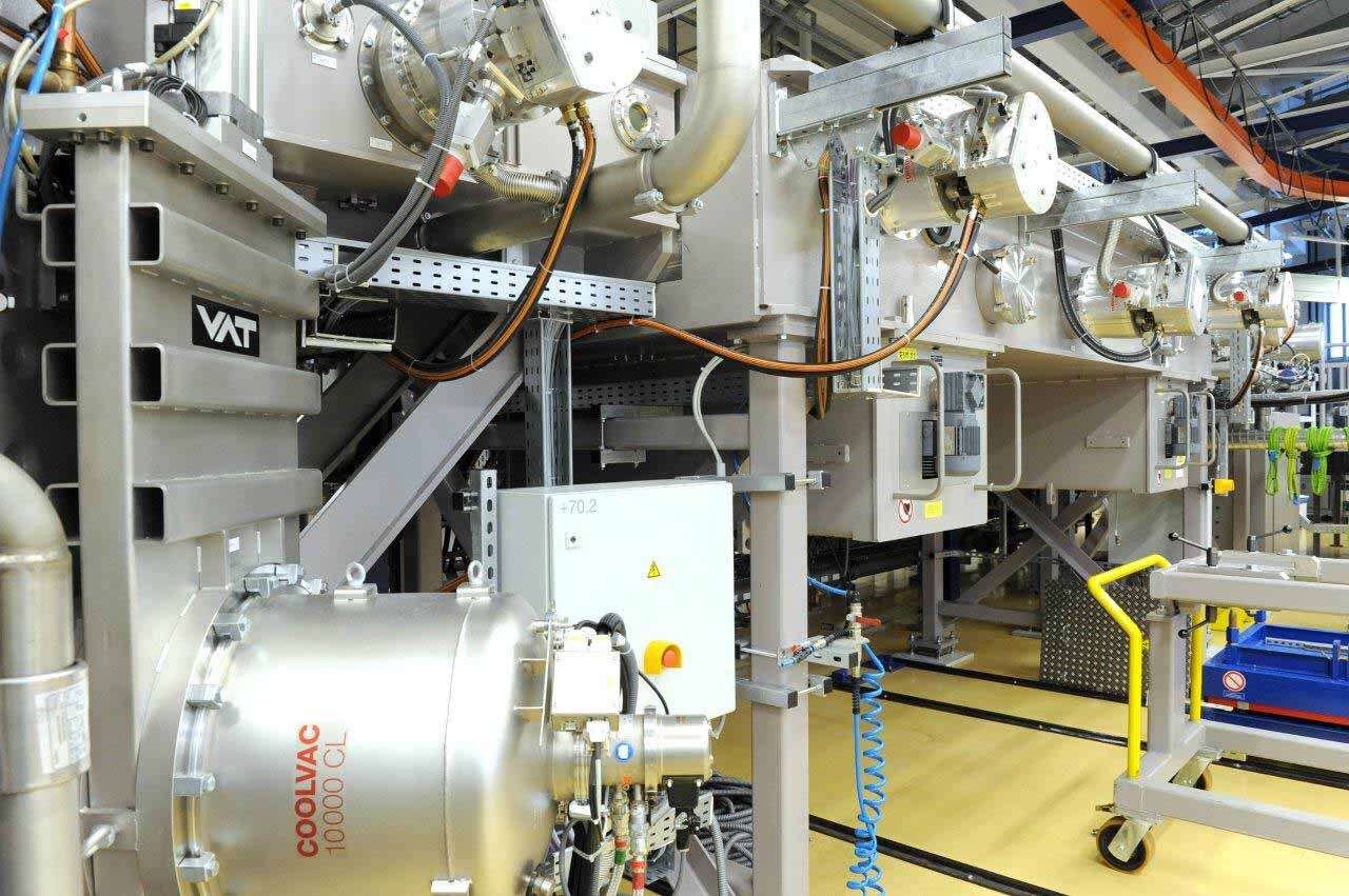
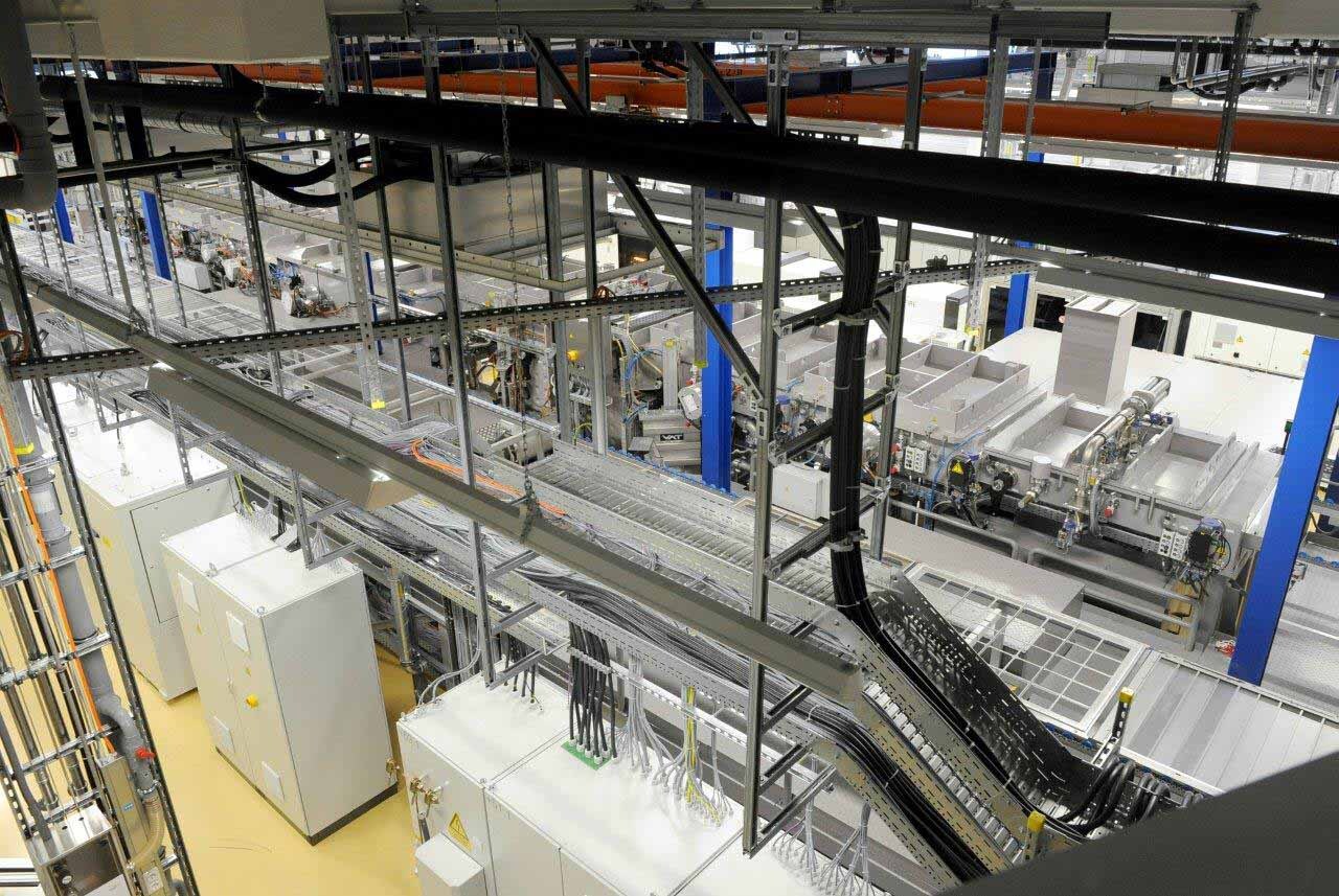
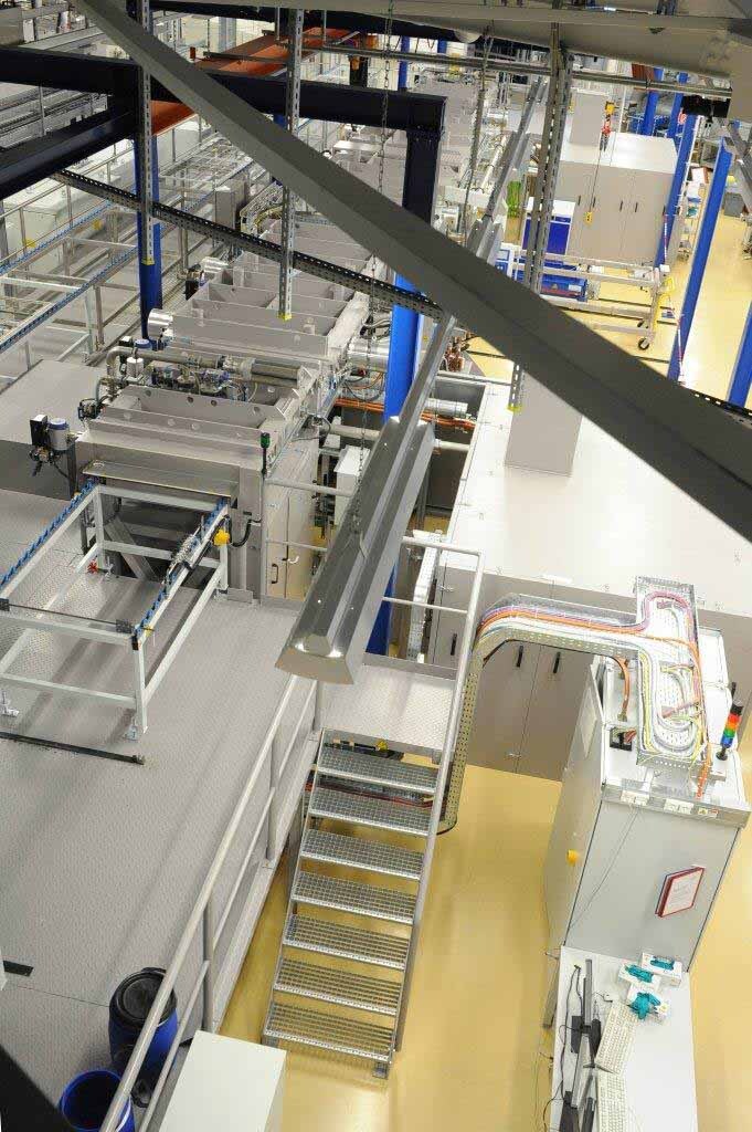
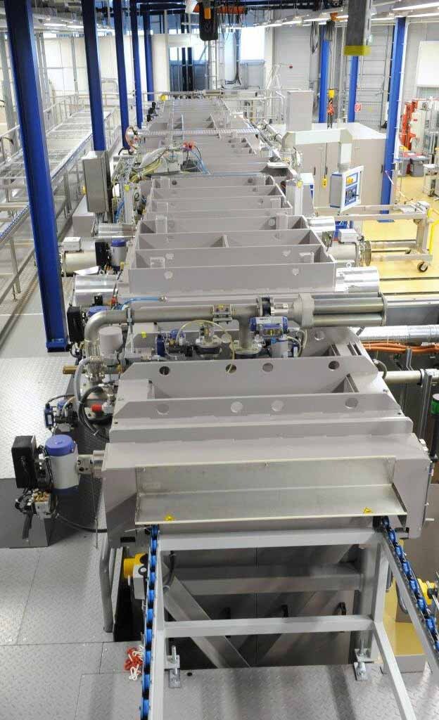
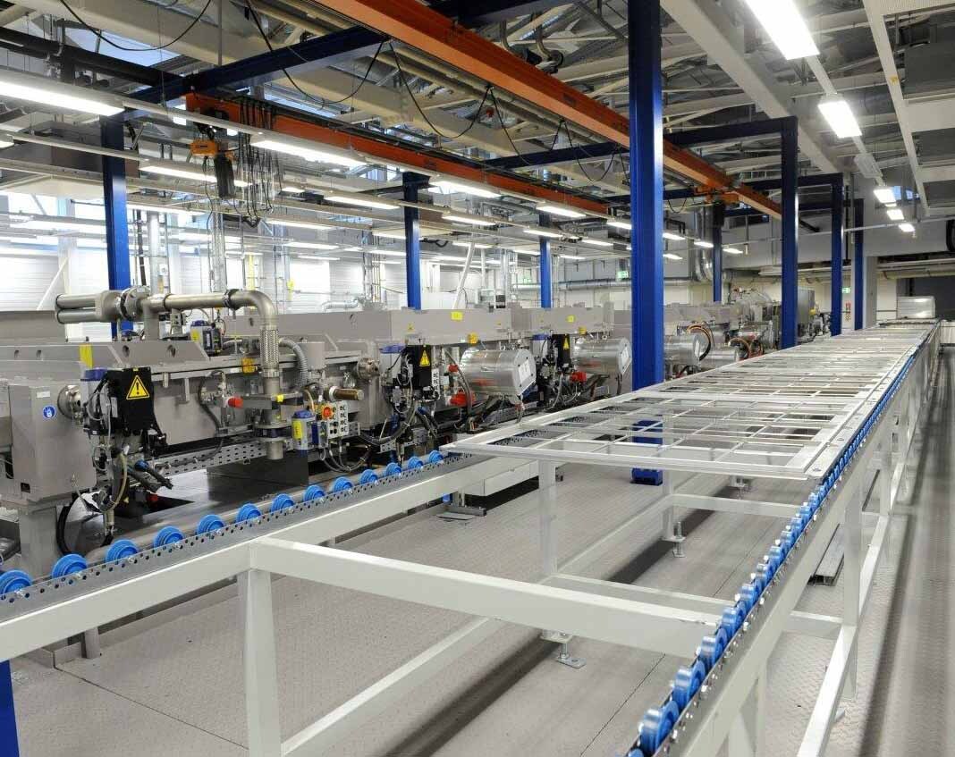
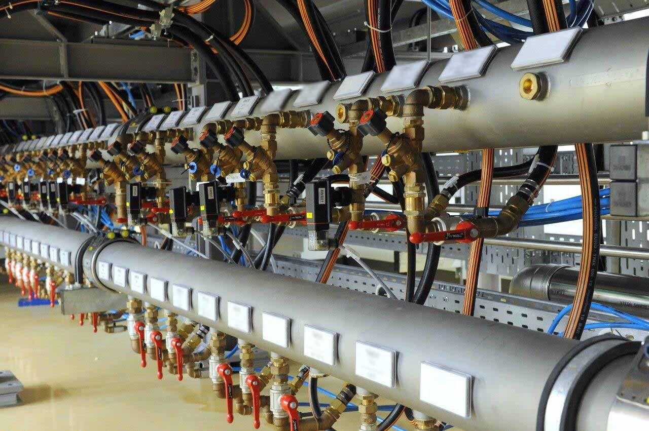
High end coating line
Wafer metallizer
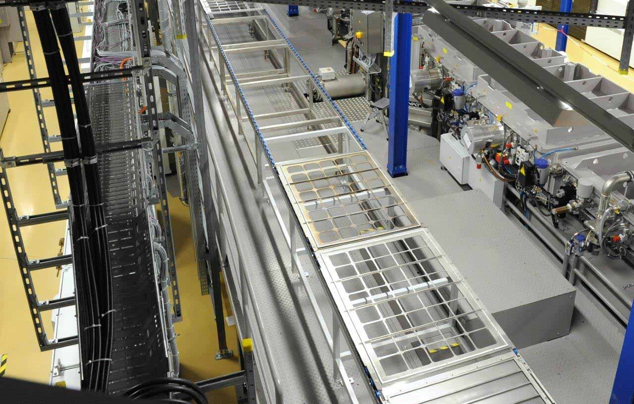
In-line complete system for coating wafers
Back coating of silicon wafers with an aluminum layer
Coating of nickel, silver and aluminum by electron beam evaporation
(35) Cells can be coated per tray
Productivity:
4,000 Wafers (5") per hour
2,600 Wafers (6") per hour
Cycle time: 50s
Technical parameters:
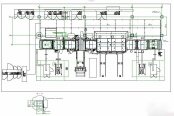
System dimensions:
Length: 19 m
Area: 20 x 7 m
Height: ~3 m
Drive:
Carrier speed max: 5 m/min
Carrier speed during vapor deposition: 1.5 - 2.0 m/min
Substrate temperature:
Max. temperature: 300°C / 572°F
Carrier dimensions:
Length: ~1,450 mm
Width: 925 mm
(60) Wafers (5") per carrier
(40) Wafers (6") per carrier
Ambient conditions:
Ambient temperature:
+15 to 35 °C
+59 to 95 °F
Relative humidity at 30°C / 86°F: < 70 %
Dust: < 10 mg/m3
Sluice chambers C1 and C7
Buffer chambers C2 and C6
Transfer chamber C5
Process chamber C4:
EB Chamber C3 / C4.1 / C4.2
Sputter chambers
(5) Sections (C4.3 to C4.7)
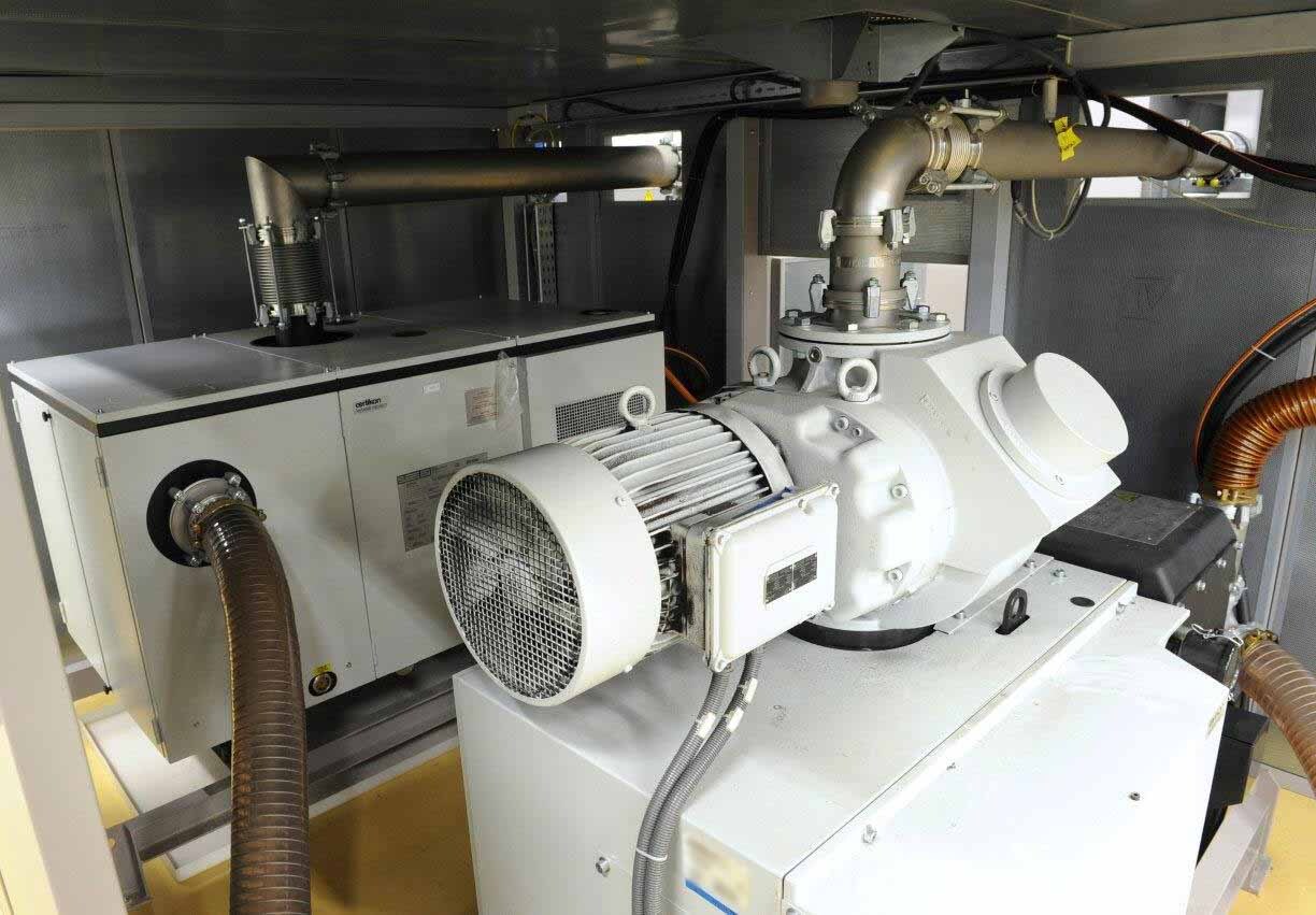
Vacuum
Working pressure:
C2 - Buffer chamber 2 to 5 x 10⁻³ mbar
C4.1 - EB chamber 5 to 9 x 10⁻⁵ mbar
C4.2 - Intermediate chamber 2 to 5 x 10⁻⁴ mbar
C4.3 - Intermediate chamber 2 to 5 x 10⁻³ mbar
C4.4 - Sputter chamber 2 to 5 x 10⁻³ mbar
C4.5 - Pump chamber 2 to 5 x 10⁻³ mbar
C4.6 - Sputter chamber 2 to 5 x 10⁻³ mbar
C4.7 - Intermediate chamber 2 to 5 x 10⁻³ mbar
C5 - Transfer chamber 2 to 5 x 10⁻³ mbar
C6 - Buffer chamber 2 to 5 x 10⁻³ mbar
Leak rate: < 1 x 10⁻² mbar l/s-1
Layer thickness / Properties:
AI with copper:
Thickness: 2 μm
Wafer thickness: > 200 μm
Temperature: 400°C / 752°F
Purity: 99.98%
AI with ceramic:
Thickness: 3 μm
Wafer thickness: 150 to 250 μm
Temperature: 300°C / 572°F
Purity: 99.5%
Ag: Thickness: < 300 nm
Sn: Thickness: < 300 nm
NiCr: Thickness: < 40 nm
Uniformity: ± 10%
Evaporation:
Production cycle: 120 h
Power of electron beam
Copper crucible: 100 to 200 kW
Ceramic crucible: 20 kW
Target material per cycle: 90 to 150 kg
Vapor utilization: 48 to 50 %
Target-substrate distance: 600 mm
Carrier frequency: 60s
Sputtering:
Target material: Ag
Target utilization: ~70%
Target life: 240 h
Cooling water:
Particle size: ~50 mg/l
pH Value: (8.0 to 9.0)
Electrical conductivity: (150 to 250) μS/cm
Acid capacity, Ks 4.3: (0.5 to 2.0) mmol/l
Filterable substances: < 50 mg/l
Chloride: < 10 mg/l
Sulfate: < 30 mg/l
Ammonium: < 0.5 mg/l
Nitrate: < 10 mg/l
Colony count (CFU): ~ 1,000 ml-1
TOC (total organic carbon): < 1.5 mg/l
Inlet temperature:
21 to 25°C
69.8 to 77°F
Differential pressure: 2 bar
Absolute pressure max: 8 bar
Water circuit 1 chambers:
Volume flow: TBD m3/h
Temperature: 25°C / 77°F
Required pressure: 6 - 8 bar
Cooling capacity: TBD kW
Electrical system:
3 Phases, 3 AC 480 V
Tolerance: -10/+6 %
Frequency: 59 to 61 Hz
Grounding resistance: <2 Ohm
Connected load max: 400 kVA
Function:
Wafers are coated on one side with (2) metal layers.
VON ARDENNE WM70H/C是一种先进的光刻设备,能够产生高质量的薄膜图像和图样。该系统设计用于创建宽度可达70 nm、高度可达100 nm的尺寸,精度可达2 nm。该单元由几个组件组成,如光掩模、光刻机、众多流体组件、气体分配器和抗蚀剂源。用于绘制晶片表面图样的光掩模首先加载到光刻机中。然后,流体组分迅速将抗蚀剂(一种化学溷合物)分配到光掩模和晶片上,并帮助均匀地扩散。然后将抗蚀剂暴露在来自洪水源的光下,以创建一个抗蚀剂模式,该模式用作模板,将在其中形成曲面细节。气体分配器精确地在抗蚀剂表面上涂抹保护性碳氟化合物薄膜,以处理气体流动并确保乳液的稠度。然后剥离、冲洗和干燥抗蚀剂,然后晶片准备进行进一步的蚀刻过程并剥离抗蚀剂。TheWM70H/C机具有市场上最先进的元件,为70-100 nm的半导体光刻工艺提供卓越的图像放置精度、精确的图样清晰度和高保真薄膜结构。当与蚀刻后谐波成像工具结合使用时,WM70H/C提供清晰、详细的功能,精度为2 nm。此外,其广泛的参数和自动化操作保证了最短的设置时间,从而显着提高了生产率。它非常适合先进半导体工艺的大批量生产环境。
还没有评论


